L293D: An H-Bridge
H-what?
An H-Bridge is nothing but an electronic circuit. Using such a circuit, you can supply current in two directions. Thats it. The L293D is an H-Bridge with two possible outputs. Meaning, you can connect two things to it... and you can control the direction of current flow in both.
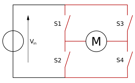
Lets say you have a DC motor, as in the diagram below:

An H-Bridge in terms of switches
If you close both S1 and S2, you'll short circuit the entire thing. Same goes with S3 and S4. Such a condition, in technical terms, is called a shoot through. So we won't consider shoot throughs.
Now, if you close switches S1 and S4, current flows through the motor from left to right. If you close S3 and S2, current flows from right to left. In these two conditions, the direction of rotation is different.
This is exactly whats needed in most robotics projects using differential drive wheels. But having physical switches would be very inconvenient. You'd need more motors to close and open switches. And to control those motors you'd need even more switches. Ah well. You probably get the point.
So what the researchers made was an electronically controlled switch: a transistor. And people used those transistors and made circuits similar to the one shown above. The only difference was that instead of physical switches, they had electronic switches.
The L293D
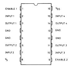
The L293D is an H-Bridge. Here's the pin-out diagram of the chip:

The pins on an L293D chip
As I had mentioned earlier, you get two output ports with the L293D. In the above pinout diagram, the left and right sides denote the two outputs. The OUTPUT1 / OUTPUT2 pair forms one output and OUTPUT3 / OUTPUT4 froms another pair. Current can flow through these pairs as dictated by the INPUT1 / INPUT2 and INPUT3 / INPUT4 pairs.
Vss is the logical voltage supply for a 1. For example, if you connect it to a 5V supply, 5 volts into any of the INPUTs would mean a logical 1. However, if you connect it to a 36V supply, the same 5 volts into any INPUT would mean a logical 0.
How did that happen? Well, you can roughly consider Vss/2 as the "threshold" for a logical 1. If a voltage is above Vss/2, then its a 1... otherwise its a 0. So for the 36V case... if any INPUT is given a voltage greater than 18V, only then will it be considered a logical 1.
Vs is the actual voltage that needs to be output. This has nothing to do with the logical 0s and 1s.
GND represents grounds. These are needed for the multiple solid state switches that are burned into the IC.
ENABLE pins enable/disable the corresponding sides. Putting a logical 1 into ENABLE1 would enable INPUT1/INPUT2 and OUTPUT1/OUTPUT2. Similarly, ENABLE2 would enable the other two input and output pins. A logical 0 disables the corresponding side.
Notice the D?
The name of the chip has a D in it... notice that? That indicates the presence of a diode for each OUTPUTx pin.
Whenever the direction of current changes, the device connected across the OUTPUT pins will resist the change. And this results in a back current. The diodes make sure that no back-current damages the circuit inside the chip or before the chip.
You could do without the diodes too (use an L293B in that case). But its recommended that you use the one with diodes, unless you know what you're doing.
Okay, so how do I make it work?
Now that you know what each pin does, explaining how to make the chip work will be easy.
Lets say you put a logical 1 into INPUT1. Then the chip will simply put Vs volts into OUTPUT1. Similarly, if you put a logical 0 into INPUT1, the chip will ground OUTPUT1.
Same thing with others. Putting a logical 1 into INPUTx will put Vs volts in OUTPUTx. And putting a 0 grounds the corresponding pin.
One word of caution though. You can use a maximum of 0.5A of current over each OUTPUTx pin. Use a bit more and you risk fusing the chip.
Conclusion
Well that it! You now know how the chip functions. You can now use it for any purpose, be it robotics or not!


